If the collector, emitter, and base of an NPN transistor are shorted together as shown in figure 5.2a, the diffusion process described earlier for diodes results in the formation of two depletion regions that surround the base as shown. The diffusion of negative carriers into the base and positive carriers out of the base results in a relative electric potential as shown in figure 5.2b.

Figure 5.2: a) NPN transistor with collector, base and
emitter shorted together, and b) voltage levels developed within the
shorted semiconductor.
When the transistor is biased for normal operation as in
figure 5.3a, the base terminal is slightly positive with
respect to the emitter (about 0.6 V for silicon), and the collector is
positive by several volts.
When properly biased, the transistor acts to make ![]() .
The depletion region at the reverse-biased base-collector junction
grows and is able to support the increased electric potential change
indicated in the figure 5.3b.
.
The depletion region at the reverse-biased base-collector junction
grows and is able to support the increased electric potential change
indicated in the figure 5.3b.
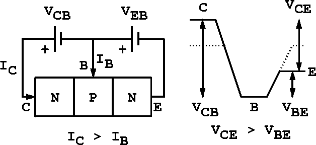
Figure 5.3: a) NPN transistor biased for operation and b)
voltage levels developed within the biased semiconductor.
For a typical transistor, 95% to 99% of the charge carriers from the
emitter make it to the collector and constitute almost all the
collector current ![]() .
.
![]() is slightly less than
is slightly less than ![]() and we may write
and we may write ![]() , where from above
, where from above ![]() to 0.99.
to 0.99.
The behaviour of a transistor can be summarized by the characteristic
curves shown in figure 5.4.
Each curve starts from zero in a nonlinear fashion, rises smoothly,
then rounds a knee to enter a region of essentially constant ![]() .
This flat region corresponds to the condition where the depletion
region at the base-emitter junction has essentially disappeared.
To be useful as a linear amplifier, the transistor must be operated
exclusively in the flat region, where the collector current is
determined by the base current.
.
This flat region corresponds to the condition where the depletion
region at the base-emitter junction has essentially disappeared.
To be useful as a linear amplifier, the transistor must be operated
exclusively in the flat region, where the collector current is
determined by the base current.

Figure 5.4: Characteristic curves of an NPN transistor.
A small current flow into the base controls a much larger current flow into the collector. We can write
![]()
where ![]() is the DC current gain and
is the DC current gain and ![]() is called the static
forward-current transfer ratio.
From the previous definition of
is called the static
forward-current transfer ratio.
From the previous definition of ![]() and the conservation of
charge,
and the conservation of
charge, ![]() , we have
, we have
![]()
For ![]() we have
we have ![]() and the transistor is a current
amplifying device.
and the transistor is a current
amplifying device.